


MANUFACTURING
2025/02/19
Behind the development of the 3D Sinter, a new technology which serves to improve both the quality of SiC power semiconductors and productivity in the manufacturing process
- Semiconductor
- Interview
- Technology
- Industrial
Index
As we see increasingly accelerating trends toward the aim to popularize EVs (electric vehicles), “SiC (silicon carbide) power semiconductors” are attracting attention as a way to contribute to the improvement of the performance of EVs.
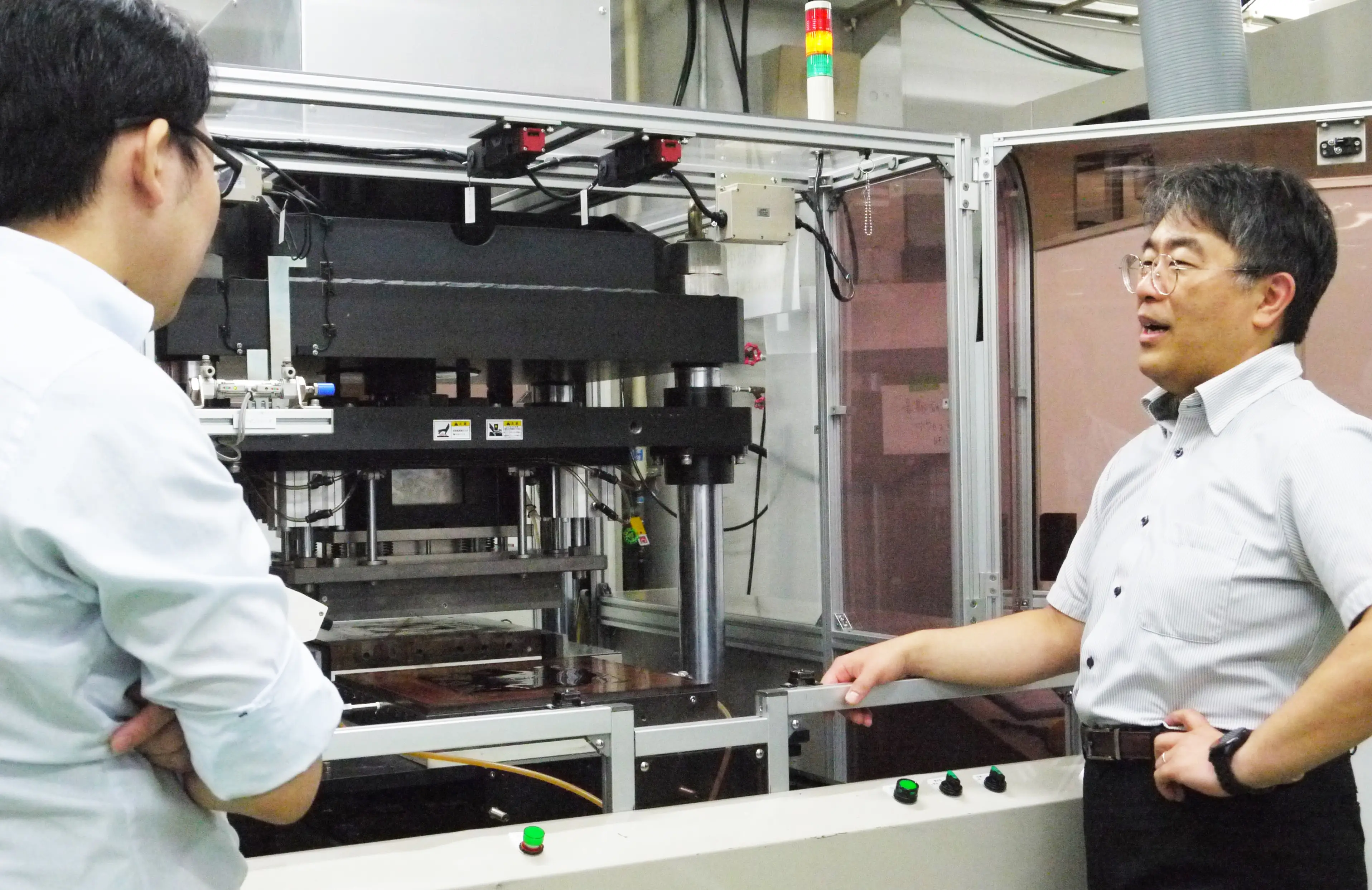
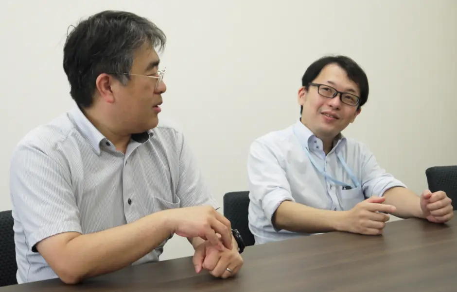
This time around, we interviewed Mr. Mori and Mr. Idesako, who are responsible for the development of the “3D Sinter,” a device that plays an important role in the manufacture of such SiC power semiconductors. We asked for details about the background of the creation of the 3D Sinter, which uses Nikkiso’s proprietary technology, the unique strengths of this piece of equipment, and the prospects for the future.
| Takahiro Mori is General Manager at the Precision Engineering Center. As an engineer, he experienced the design, development, and customer-side implementation of equipment, including the predecessor of the 3D Sinter. He is currently responsible for the engineering management of manufacturing equipment for the manufacture of electronic components, water-conditioning systems for power plants, and so on. Satoshi Idesako is in charge of the development of equipment, test support for customers, and other such areas at the Precision Engineering Center. *Affiliations and titles are current as of the time of the interview. |
Nikkiso’s proprietary 3D Sinter technology contributes to the improved quality of power semiconductors
—— Thank you very much for your time today. First of all, could you explain what a “sintering device” is?
Idesako: Recently, SiC power semiconductors have been attracting attention as next-generation semiconductor devices that can withstand higher voltages and apply larger electrical currents than conventional semiconductors.
The process of bonding chips on substrates using bonding materials made of silver or copper when manufacturing these SiC power semiconductors is called “sintering.” Sintering equipment is used to bond chips and substrates using heat and pressure.
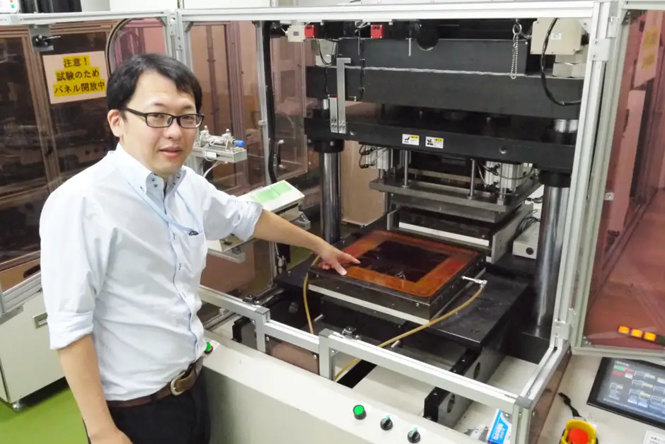
—— Can you tell us about the 3D Sinter developed by Nikkiso? How does it differ from a conventional device?
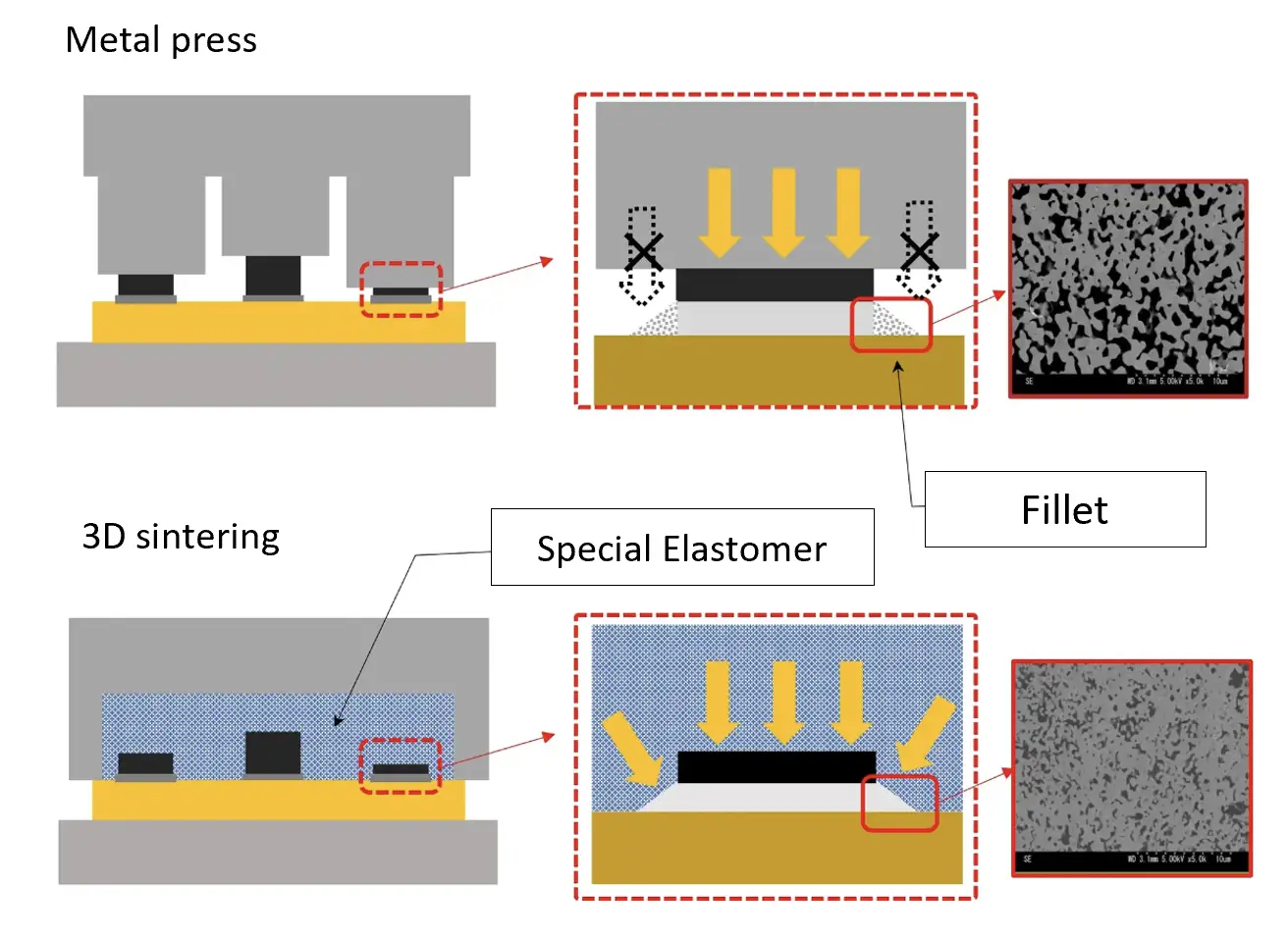
Idesako: With the conventional “metal press method,” the die that pressed the chip consisted of a flat plate, with the chip then being pressed flat from directly above.
In contrast, 3D Sintering deploying the usage of Nikkiso’s proprietary technology known as the “3D press method,” involves the usage of a special soft gel-like pressurizing medium (elastic body) in the pressurizing section. The mechanism involves this medium being wrapped around the chip on the substrate.
—— Can you tell us about the some of the advantages of using this 3D Sinter?
Idesako: First of all, unevenness in terms of pressure can be eliminated.
With a conventional sintering device, the pressure can be higher or lower than specified depending on the chip height, or there can be differences present in terms of pressure between the center and the edge of the area to be pressurized, resulting in pressure irregularities.
The 3D Sinter, on the other hand, involves pressing in manner that follows the unevenness of the chip, so uniform pressure is applied to all areas. This eliminates the possibility of some parts not being pressed properly or the possibility of too much pressure causing chips to crack.
It is true that even with the conventional methods, it is possible to eliminate pressure irregularities through the usage of molds that are appropriate for the shape of the chip. However, with this method, the mold must be remade for each type of chip. The use of a 3D Sinter can reduce the time and labor required for this process, as well as eliminate the need to produce expensive molds for each type of chip, thereby significantly reducing running costs.
In addition, the 3D Sinter helps to increase the strength of SiC power semiconductors.
In the past, only flat pressure was applied to the chip area, so pressure was not applied to the area where the bonding material protruded from between the chip and substrate (fillet area). In other words, there was concern that the chips would peel off from this edge, which was not baked firmly in place.
The 3D Sinter, on the other hand, wraps around the entire chip and applies pressure from each direction, increasing the strength of the fillet area and reducing the risk of chip delamination.
We want to be ahead of the market trends and translate new technologies into reality
—— What kind of process led up to the development of the 3D Sinter?
Mori: We did not start out developing equipment for SiC power semiconductors, but rather found one application during the process of applying a three-dimensional pressing technology using water pressure in the pressure bonding process of MLCCs (multilayer ceramic capacitors).
The “nano-silver” and “nano-copper” materials currently used as bonding materials have been attracting attention for the high levels of heat resistance and durability which they provide. Since these sintering temperatures exceed 300 degrees Celsius, our thinking was that technology to press at temperatures exceeding 300 degrees Celsius was likely to be required in the future. In fact, in the area of SiC power semiconductors, where the operating environment involves high temperatures, nano-silver and nano-copper have come to replace solder, which was once the mainstream material.
However, elastic materials, which are organic, can withstand temperatures up to 200 degrees Celsius. At first, we did not have a concrete image of how we could create a device that could press at an ultra-high temperature of 300 degrees Celsius. We started this technology development project for finding a technology that would enable uniform pressurization at 300 degrees Celsius and put us ahead of the trends in the market.
—— What kind of technology came about and led to the birth of the 3D Sinter?
Idesako: We tried to devise materials and mold structures for the elastic material, but we could not find a material that was both soft enough to follow unevenness and strong enough to withstand heat and pressure, nor could we find a structure that could apply uniform pressure. It took about six months of continuous trial and error to find such a material. Then, unexpected inspiration led to the idea of “heating only the area that we wanted to have heated” (meaning the junction surface of the substrate and the chip).
Mori: It meant going from a method wherein the entire mold is heated to 200 degrees Celsius to one wherein the upper portion of the mold, including the elastic body, is not heated, but the temperature of the workpiece under pressure is increased to 300 degrees Celsius. It would also involve soft insulation layer being added between the bonding material and the elastic body. This prevents the elastic material from becoming hotter than 200 degrees Celsius while at the same time creating a state where heat is concentrated in the area to be pressurized, thereby realizing a press at a temperature of 300 degrees Celsius.
Furthermore, preparing two molds, one for heating and one for cooling, and switching them, allows for rapid cooling to take place while pressing, which was something difficult to do in the past. In addition, the risk of the temperature of the elastic material rising during the pressing process has been eliminated, bringing the product closer to practical application.
This technology took shape about two years after we began developing it. As we proceeded with tests and demonstrations, we realized that we could apply this technology to sintering as well. Thus, the 3D Sinter was born.
—— What were both of your thoughts when the technology was being developed?
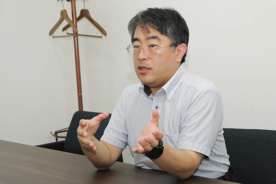
Mori: With most technical development projects, we have a vague idea of what we want to do and then proceed with the idea. This time, however, we had no idea at all in that sense. The time spent pondering what to do until we arrived at a feasible idea was painful at times.
The breakthrough idea of “heating only the area that we wanted to have heated” just happened to occur to me while I was warming myself in the bath. From there, development began to accelerate once again. I am glad that I was able to follow through developing what I said that I would.
Idesako: In the course of responding to customer demonstrations and tests, I also heard requests from customers for higher pressing temperatures and greater pressure levels. I wanted to do something about that. We have been undertaking development with the hope that we can have Nikkiso’s equipment, and by extension the cooperation of our engineering centers, serve to solve the issues that our customers are facing.
I heard about Mr. Mori’s idea when I happened to meet him while I was out of the office. It was something I had not thought about at all, but I felt like it opened up a path that I had been stuck on. I felt like this was sure what would make things work in that sense.
Demonstration sites are quickly being set up in China, where the power semiconductor market is booming
—— I have heard that after installing a demo unit of the 3D Sinter in Japan, you opened a demo room in Shanghai in January 2023. Can you tell us about the background behind the expansion into Shanghai?
Mori: We urgently needed to create a place to test our equipment in China, where the power semiconductor market is even more vibrant than in Japan.
Chinese customers, in particular, are often not convinced by presentations alone. Since it was necessary to prove that power semiconductor sintering “could be done” right then and there, we brought the equipment to Shanghai and opened a demonstration room.
Idesako: Joining materials are essentially raw materials in the sense that they should be applied, dried immediately, and then pressed right on the spot. We needed a local base where we could give demonstrations in response to customer requests in a timely manner, without having to bring or send materials to the site each time.
—— How is the demo room in Shanghai and how has the customer response been?
Idesako: There are still a certain number of needs that exist when it comes to demonstrations, and we continuously conduct one or two demonstrations per week, proceeding from the briefing to the preparation of materials, and the determination of conditions.
In the past, we had mainly introduced our products overseas using documents. We are now receiving favorable feedback from our customers because they can now get a concrete image of the size and configuration of the equipment by standing in front of the actual product. And, as one would expect, some great feedback we’ve received with respect to our ability to provide a timely response to requests, was in the form of a comment to the effect that the customer was glad to have had a demonstration provided immediately.
The development of technology continues so that we can meet the demands of more customers
——Thank you very much. Finally, what are your thoughts when it comes to the future?
Idesako: While I am glad that this device has taken shape, I wonder if we are still merely at the starting line. As we proceed with the demonstrations, we are receiving requests for further improvements, and we would like to continue brushing things up more and more.
Currently, we are developing equipment to meet customer requirements for the mass manufacturing of power semiconductors, and we hope to continue development to further increase productivity in the future.
Mori: This new technology, which has made the previously impossible possible, is being developed based on a product-oriented concept, so it is necessary to create applications going forward.
We would like to take on the challenge of the development of applications to meet the demands of more customers. That means when it comes to the nano-silver and nano-copper introduced this time, and in the next stage, aim for application to “heat dissipation substrates” used for parts with large amounts of heat generation.
この記事をシェアする
Pickup
-
 MEDICAL FIELD
Empowering Asia’s Expanding Dialysis Treatment with Nikkiso’s Advanced Technology and Comprehensive Support
- Hemodialysis
- Interview
- Medicalbusiness
2025/10/30
-
 MANUFACTURING
Pumps also actively used in semiconductor manufacturing: 20 years of history of compact, high-speed canned motor pumps
- Technology
- Interview
- Pump
- Semiconductor
2025/05/21
-
 MANUFACTURING
Nikkiso's DX initiatives: CAE Support Department continues to evolve, aiming to eliminate dependence on the skills and expertise of specific people
- Technology
- Interview
2025/04/09
PICK UP
-
Empowering Asia’s Expanding Dialysis Treatment with Nikkiso’s Advanced Technology and Comprehensive Support
-
Pumps also actively used in semiconductor manufacturing: 20 years of history of compact, high-speed canned motor pumps
-
Nikkiso's DX initiatives: CAE Support Department continues to evolve, aiming to eliminate dependence on the skills and expertise of specific people
-
A region on the forefront of dialysis treatment: Nikkiso automation gathering attention in Europe
-
Behind the development of the 3D Sinter, a new technology which serves to improve both the quality of SiC power semiconductors and productivity in the manufacturing process